- 您现在的位置:买卖IC网 > Sheet目录488 > NTD5865N-1G (ON Semiconductor)MOSFET N-CH 60V 34A 18MOHM DPAK
�� �
�
�NTD5865N�
�N-Channel� Power� MOSFET�
�60� V,� 43� A,� 18� m� W�
�Features�
�?� Low� Gate� Charge�
�?� Fast� Switching�
�?� High� Current� Capability�
�?� 100%� Avalanche� Tested�
�?� These� Devices� are� Pb� ?� Free,� Halogen� Free� and� are� RoHS� Compliant�
�MAXIMUM� RATINGS� (T� J� =� 25� °� C� unless� otherwise� noted)�
�V� (BR)DSS�
�60� V�
�http://onsemi.com�
�R� DS(on)� MAX�
�18� m� W� @� 10� V�
�I� D� MAX�
�43� A�
�Parameter�
�Drain� ?� to� ?� Source� Voltage�
�Gate� ?� to� ?� Source� Voltage� ?� Continuous�
�Gate� ?� to� ?� Source� Voltage�
�?� Non� ?� Repetitive� (t� p� <� 10� m� s)�
�Symbol�
�V� DSS�
�V� GS�
�V� GS�
�Value�
�60�
�"� 20�
�"� 30�
�Unit�
�V�
�V�
�V�
�G�
�D�
�Current� (R� q� JC� )�
�Power� Dissipation�
�T� C� =� 25� °� C�
�Continuous� Drain� T� C� =� 25� °� C�
�Steady� T� C� =� 100� °� C�
�State�
�(R� q� JC� )�
�Pulsed� Drain� Current� t� p� =� 10� m� s�
�Operating� Junction� and� Storage� Temperature�
�I� D�
�P� D�
�I� DM�
�T� J� ,� T� stg�
�43�
�31�
�71�
�192�
�?� 55� to�
�175�
�A�
�W�
�A�
�°� C�
�S�
�N� ?� CHANNEL� MOSFET�
�4�
�4�
�3�
�Source� Current� (Body� Diode)�
�Single� Pulse� Drain� ?� to� ?� Source� L� =� 0.1� mH�
�Avalanche� Energy�
�Lead� Temperature� for� Soldering� Purposes�
�(1/8� ″� from� case� for� 10� s)�
�I� S�
�E� AS�
�I� AS�
�T� L�
�43�
�36�
�27�
�260�
�A�
�mJ�
�A�
�°� C�
�1� 2�
�3�
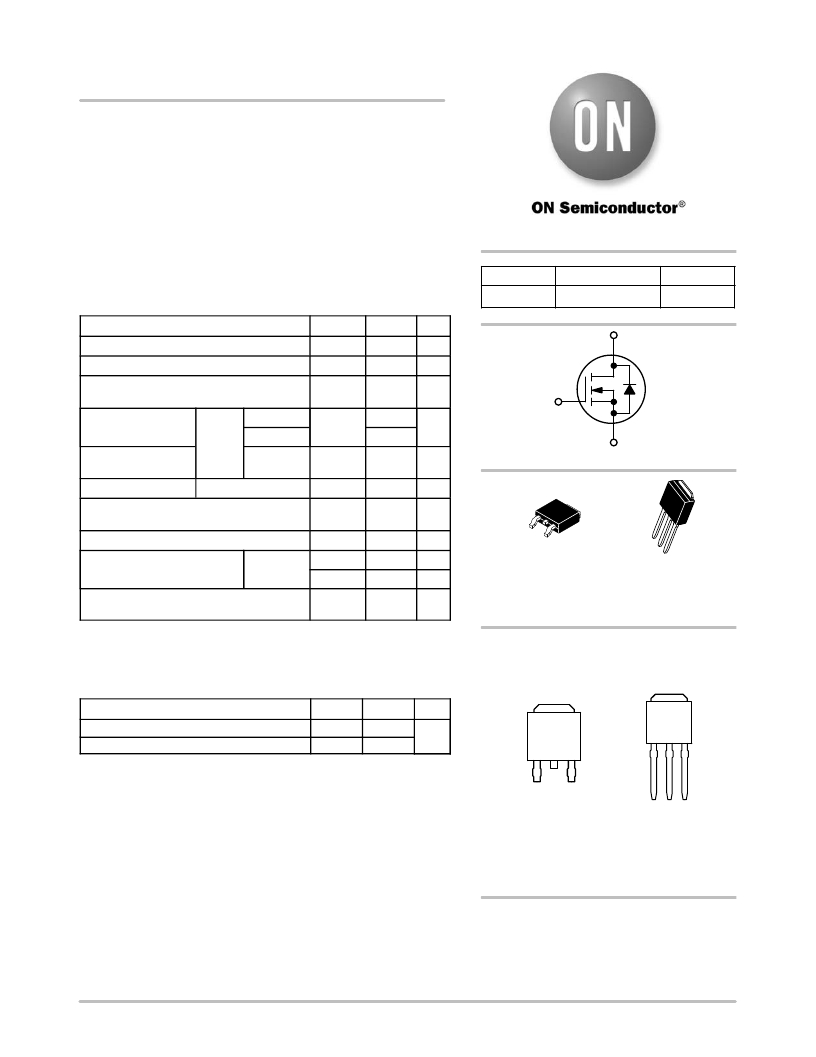
�DPAK�
�CASE� 369C�
�(Surface� Mount)�
�STYLE� 2�
�1�
�2�
�IPAK�
�CASE� 369D�
�(Straight� Lead)�
�STYLE� 2�
�Stresses� exceeding� Maximum� Ratings� may� damage� the� device.� Maximum�
�Ratings� are� stress� ratings� only.� Functional� operation� above� the� Recommended�
�Operating� Conditions� is� not� implied.� Extended� exposure� to� stresses� above� the�
�Recommended� Operating� Conditions� may� affect� device� reliability.�
�THERMAL� RESISTANCE� MAXIMUM� RATINGS�
�Parameter� Symbol� Value� Unit�
�MARKING� DIAGRAMS�
�&� PIN� ASSIGNMENT�
�4�
�4� Drain�
�Drain�
�Junction� ?� to� ?� Case� (Drain)�
�R� q� JC�
�2.1�
�°� C/W�
�Junction� ?� to� ?� Ambient� ?� Steady� State� (Note� 1)� R� q� JA� 49�
�1.� Surface� ?� mounted� on� FR4� board� using� a� 650� mm� 2� ,� 2� oz.� Cu� pad.�
�2�
�1� Drain� 3�
�Gate� Source�
�1� 2� 3�
�Gate� Drain� Source�
�Y�
�WW�
�5865N�
�G�
�=� Year�
�=� Work� Week�
�=� Device� Code�
�=� Pb� ?� Free� Package�
�ORDERING� INFORMATION�
�See� detailed� ordering� and� shipping� information� in� the� package�
�dimensions� section� on� page� 2� of� this� data� sheet.�
�?� Semiconductor� Components� Industries,� LLC,� 2013�
�January,� 2013� ?� Rev.� 2�
�1�
�Publication� Order� Number:�
�NTD5865N/D�
�发布紧急采购,3分钟左右您将得到回复。
相关PDF资料
NTD5865NL-1G
MOSFET N-CH 60V 40A 16MOHM IPAK
NTD5867NL-1G
MOSFET N-CH 60V 18A 43MOHM IPAK
NTD60N02RT4
MOSFET N-CH 25V 8.5A DPAK
NTD6414ANT4G
MOSFET N-CH 100V 32A DPAK
NTD6415ANLT4G
MOSFET N-CH 100V 23A 56MOHM DPAK
NTD6415ANT4G
MOSFET N-CH 100V 23A DPAK
NTD6416AN-1G
MOSFET N-CH 100V 17A IPAK
NTD6416ANL-1G
MOSFET N-CH 100V 19A DPAK
相关代理商/技术参数
NTD5865NL
制造商:ONSEMI 制造商全称:ON Semiconductor 功能描述:N-Channel Power MOSFET 60 V, 40 A, 16 mΩ
NTD5865NL-1G
功能描述:MOSFET Single N-CH 60V 40A RoHS:否 制造商:STMicroelectronics 晶体管极性:N-Channel 汲极/源极击穿电压:650 V 闸/源击穿电压:25 V 漏极连续电流:130 A 电阻汲极/源极 RDS(导通):0.014 Ohms 配置:Single 最大工作温度: 安装风格:Through Hole 封装 / 箱体:Max247 封装:Tube
NTD5865NLT4G
功能描述:MOSFET Single N-CH 60V 40A RoHS:否 制造商:STMicroelectronics 晶体管极性:N-Channel 汲极/源极击穿电压:650 V 闸/源击穿电压:25 V 漏极连续电流:130 A 电阻汲极/源极 RDS(导通):0.014 Ohms 配置:Single 最大工作温度: 安装风格:Through Hole 封装 / 箱体:Max247 封装:Tube
NTD5865NT4G
功能描述:MOSFET Single N-CH 60V 38A RoHS:否 制造商:STMicroelectronics 晶体管极性:N-Channel 汲极/源极击穿电压:650 V 闸/源击穿电压:25 V 漏极连续电流:130 A 电阻汲极/源极 RDS(导通):0.014 Ohms 配置:Single 最大工作温度: 安装风格:Through Hole 封装 / 箱体:Max247 封装:Tube
NTD5867NL
制造商:ONSEMI 制造商全称:ON Semiconductor 功能描述:N-Channel Power MOSFET 60 V, 20 A, 39 m
NTD5867NL-1G
功能描述:MOSFET NFET DPAK 60V 18A 43 MOHM RoHS:否 制造商:STMicroelectronics 晶体管极性:N-Channel 汲极/源极击穿电压:650 V 闸/源击穿电压:25 V 漏极连续电流:130 A 电阻汲极/源极 RDS(导通):0.014 Ohms 配置:Single 最大工作温度: 安装风格:Through Hole 封装 / 箱体:Max247 封装:Tube
NTD5867NLT4G
功能描述:MOSFET NFET DPAK 60V 18A 43 MOHM RoHS:否 制造商:STMicroelectronics 晶体管极性:N-Channel 汲极/源极击穿电压:650 V 闸/源击穿电压:25 V 漏极连续电流:130 A 电阻汲极/源极 RDS(导通):0.014 Ohms 配置:Single 最大工作温度: 安装风格:Through Hole 封装 / 箱体:Max247 封装:Tube
NTD5N50
制造商:Rochester Electronics LLC 功能描述:- Bulk 制造商:Motorola Inc 功能描述: 制造商:ON Semiconductor 功能描述: 制造商:MOTOROLA 功能描述: